← T8 Ballast Wiring Diagram: Master Your Lighting Setup! T8 ballast wiring diagram parallel Rheostat Switch Wiring Diagram: Master Your Dimmer Setup! How to wire a 3 way dimmer switch diagrams 3-way wiring inst →
If you are searching about How to Reduce Ground Bounce: Mitigating Noise with PCB Design Best you've visit to the right web. We have 25 Images about How to Reduce Ground Bounce: Mitigating Noise with PCB Design Best like Reducing Ground Bounce in PCB Assembly | Sierra Circuits, Ground Bounce Reduction Techniques for PCB Signal Integrity Issues and also Understanding Signal Integrity in PCBs | Sierra Circuits. Here it is:
How To Reduce Ground Bounce: Mitigating Noise With PCB Design Best
.jpg) sosteneslekule.blogspot.com
sosteneslekule.blogspot.com
bounce ground pcb noise reduce mitigating practices design
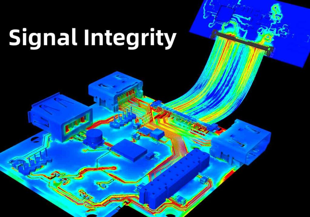
What Is Signal Integrity? A Comprehensive Overview - RayMing PCB
 www.raypcb.com
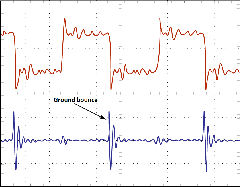
How Ground Bounce Can Ruin Your Day - An Example With An LCD Display
 www.signalintegrityjournal.com
ground bounce ruin integrity lcd 1591 signalintegrityjournal
How Ground Bounce Can Ruin Your Day - An Example With An LCD Display
 www.signalintegrityjournal.com
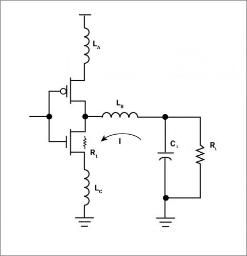
bounce ruin probe inductance method
Ground Bounce Reduction Techniques For PCB Signal Integrity Issues
How To Reduce Ground Bounce In PCB Assembly
 hyperedge.tech
How To Reduce Ground Bounce In PCB Assembly
 hyperedge.tech
What Is Signal Integrity? A Comprehensive Overview - RayMing PCB
 www.raypcb.com
How To Improve Signal Integrity In PCB Design (Guidelines) - Artist 3D
 artist-3d.com
How To Reduce Ground Bounce: Mitigating Noise With PCB Design Best
.jpg) www.allaboutcircuits.com
www.allaboutcircuits.com
bounce ground pcb noise mitigating reduce practices design articles vias decoupling tied planes capacitors should power
How To Reduce Ground Bounce: Mitigating Noise With PCB Design Best
 www.allaboutcircuits.com
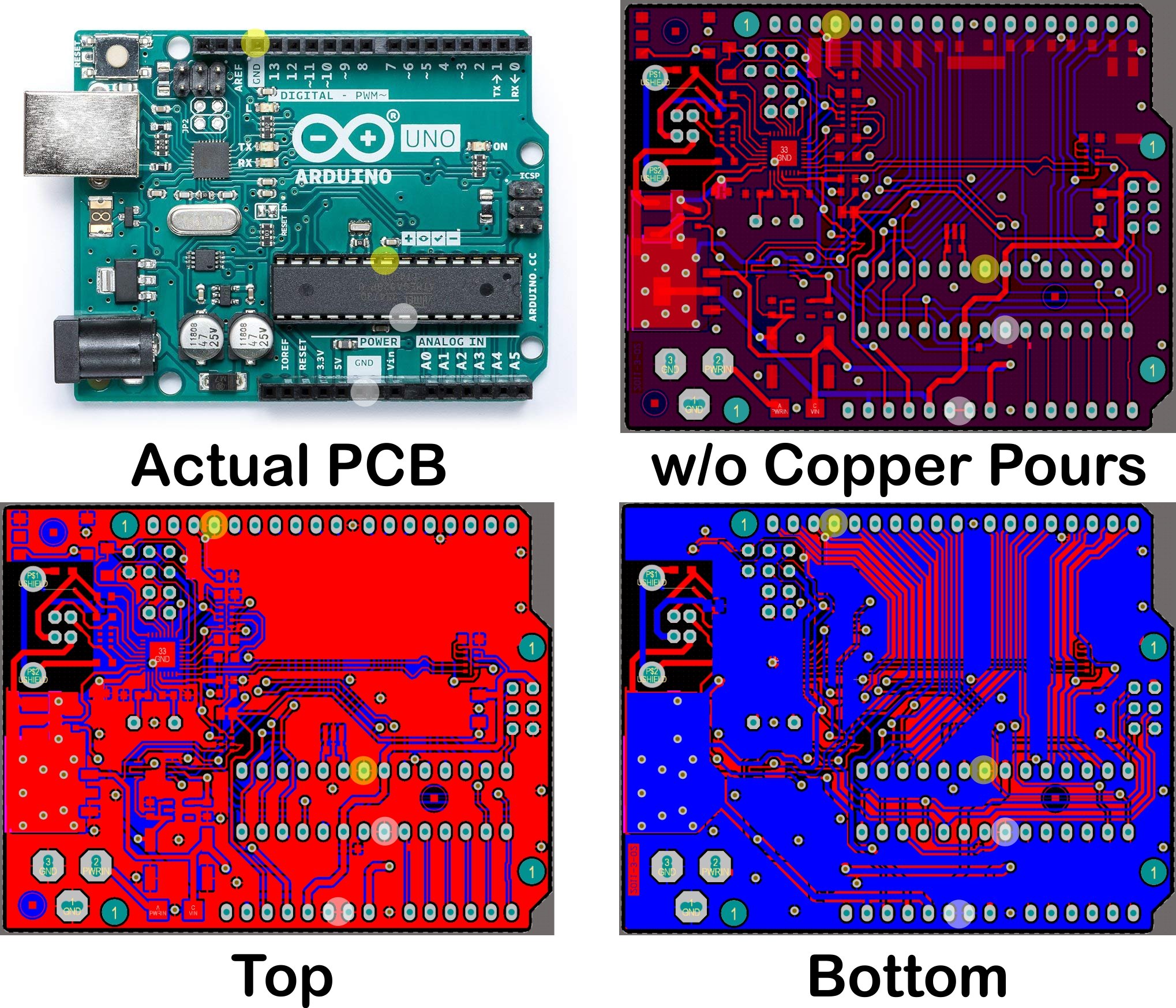
ground pcb bounce noise design analog mitigating practices reduce articles highlighted respectively yellow digital white
Ground Bounce Reduction Techniques For PCB Signal Integrity Issues
How To Improve Signal Integrity In PCB Design (Guidelines) - Artist 3D
 artist-3d.com
Signal Integrity - PCB Considerations During The Circuit Design
 www.epectec.com
signal integrity pcb circuit design schematic depicting printed board epectec
Signal Integrity-How To Do It In PCB Design?
 www.wellpcb.com
Reducing Ground Bounce In PCB Assembly | Sierra Circuits
 www.protoexpress.com
How To Reduce Ground Bounce: Mitigating Noise With PCB Design Best
 www.allaboutcircuits.com
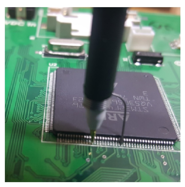
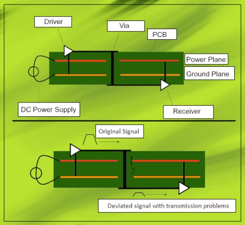
ground pcb bounce noise black reduce practices mitigating design beaglebone articles evaluation instruments texas kit captured attached cape figure
Understanding Signal Integrity In PCBs | Sierra Circuits
 www.protoexpress.com
Ground Bounce Reduction Techniques For PCB Signal Integrity Issues
 resources.altium.com
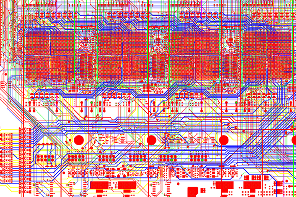
9 Factors That Lead To Signal Integrity Issues In A PCB | Sierra Circuits
 www.protoexpress.com
integrity pcb transmission issues lead
Guide To Signal Integrity Analysis In PCB Design | NWES Blog
 www.nwengineeringllc.com
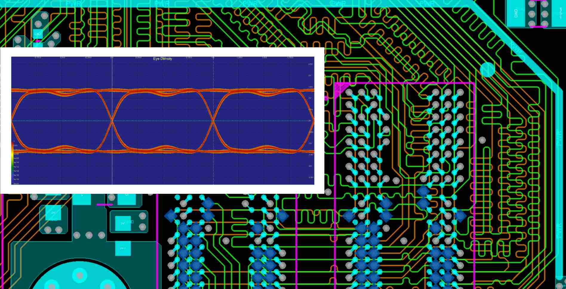
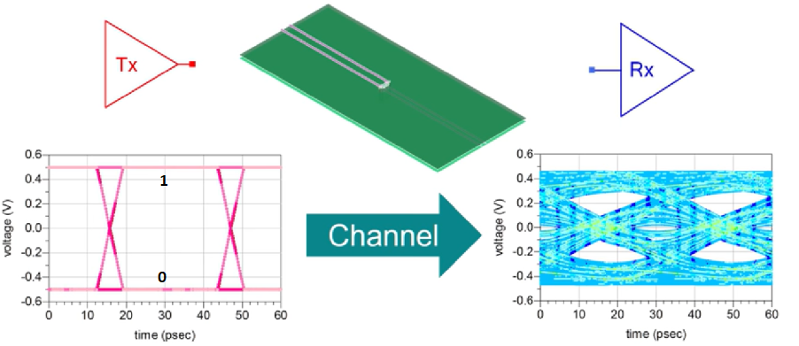
signal integrity pcb analysis design capacitors decoupling eye diagram what capacitor resonances simulations parasitics produce include included self own need
How To Reduce Ground Bounce: Mitigating Noise With PCB Design Best
 www.allaboutcircuits.com
ground bounce pcb noise reduce mitigating practices design articles pull push circuit figure
Reducing Ground Bounce In PCB Assembly | Sierra Circuits
 www.protoexpress.com
Signal Integrity - PCB Considerations During The Circuit Design
 www.epectec.com
signal integrity pcb circuit schematic depicting printed board si epectec
Signal Integrity-How To Do It In PCB Design?
 www.wellpcb.com
integrity signal pcb wellpcb
Signal integrity-how to do it in pcb design?. How to reduce ground bounce: mitigating noise with pcb design best. How to improve signal integrity in pcb design (guidelines)